Introduction
Ultraviolet (UV) irradiation is defined as a type of electromagnetic radiation, with a wavelength (100–400nm) shorter than that of visible light (400–700nm), but longer than x-rays (<100 nm)[1]. Ultra Violet C irradiation (UVC) ranges from 100 to 280nm in wavelength. UV irradiation is divided into four distinct spectral areas including vacuum UV (100–200 nm), UVC (200–280 nm), UVB (280–315 nm) and UVA (315–400 nm)[2].
Due to its power to damage the genetic material (DNA and RNA) of microorganisms, which can prevent them from producing, UVC irradiation is widely used in disinfection and sterilization. Besides, a variety of molecules exhibit autofluorescence with UV light excitation. So UVC is widely used in the field of medicine and biology[3].
Because of UVC’s excellent bioluminescent properties, it can be used in medical and biological sensing. Meanwhile, UVC has a short wavelength, which means it can have a good resolution in optical imaging[4].
This paper starts with the application of this direction. Efficient collection of information carrying UVC light means related devices can be miniaturized and integrated. To be applied to around the wavelength with 266 nm, a design scheme for grating couplers based on the \(SiO_2\) is presented in this paper.
The paper starts with an introduction to the approach we used for our simulation. Next, we proposed the calculation for the initial parameter during the design. Then we move to the simulation, analyze the result, try to improve it and verify the improved proposals. Finally, we will have a conclusion about the whole project.
FDTD
To design a photonic device, we are required to understand how light will propagate in the structure. Considering reflections, interference, scattering and radiation, interaction between multiple modes, changes in the mode profile and so on variations of light, we need an approach to solve how the light will propagate in our design.
In this project, we mainly use the Lumerical to help us do the simulation. To be more specific, it is the finite difference time domain (FDTD) method that we used for the simulation. So we will talk about the FDTD method first in this chapter[5].
FDTD or so-called Yee’s method is a general and rigorous approach to solving how waves propagate. It is a typical numerical method for solving the electromagnetic wave equation in the time domain, by applying finite difference approximations to the related system of differential equations. This grid-based differential numerical modelling method is based on Maxwell equations or the scalar Helmholtz equation[6].
FDTD is a grid-based differential numerical modelling method. To easily calculate, this method will discretize the physical quantities of the nanostructure we want to simulate. Such discretization can be uniform or non-uniform mesh, which makes it can adjust the precision of mesh, and then adjust the computing resources and computing speed. Normally speaking, the higher the mesh accuracy, the smaller the basic cells and more accurate results, but at the expense of much more time for calculating. Besides, free discretization can make the simulation more accurate, since we can set more meshed in the interface or structure we are interested in[7].
FDTD is widely used in silicon photonics because of the following benefits:
- Convenient for large-scale simulations.
- Reliable for broadband and transient simulations.
- Accurate, robust, and mature which was proven in various fields.
- Easy to debug.
- Great for researching electromagnetics behaviours
Grating Design
A grating coupler is a kind of periodic structure, which can diffract light between the waveguide and free space. Due to that, it can be used as an I/O component, whose goal is to couple light between free space or fibre and waveguide[8]. To get a better coupling efficiency, and couple light as much as possible, we need to adjust the relevant parameters of the grating coupler according to the demand calculation[9].
Parameter calculation
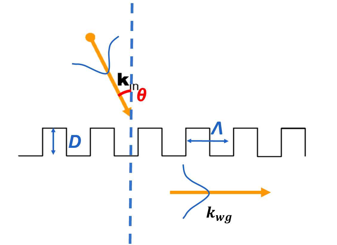
The figure above shows the cross-section schematic of a grating coupler. Such a grating coupler usually consists of a silicon waveguide core, a top cladding using oxide or air, a bottom cladding using buried oxide as the substrate, and a silicon substrate.
Considering the situation that an arbitrary wave propagates in a uniform medium, it can be seen as a set of plane waves which propagate independently without power exchange. The plane waves will be diffracted when the medium has a periodic structure. Such periodic structure leads to very specific coupling between certain plane waves of the set (or between specific directions), which is described by the so-called Bragg condition. Hence, we can couple an incident light (usually guided by a fibre) propagate through the waveguide, and use the light to convey information to achieve our goals.
Bragg condition relates to the k-vector of the incident plane wave and the k-vectors of the diffraction orders. Therefore, we can use a k-vector diagram as a handy tool to easily graphically depict the relationship between the k-vectors, and calculate the parameters which influence the coupling efficiency.
There are several important grating coupler parameters shown in Figure1 to determine the coupling efficiency[10]:
- Λ is the period of the grating
- D is the etch depth of the grating
- The duty cycle, or fill factor, is the etch width divided by the period
- θ is the angle between the surface normal and the propagation direction of incident light
To design a waveguide grating coupler, we need to simulate different situations with different parameters and select the optimal parameters from them. In our project, the light beam we want to couple will incident at an angle of 10° from the surface normal. The centre wavelength is around 266nm. In the meantime, the material we used to build the grating coupler is Silica(\(SiO_2\)). Through these target demands and known quantities, we can draw such k-diagram as follows:
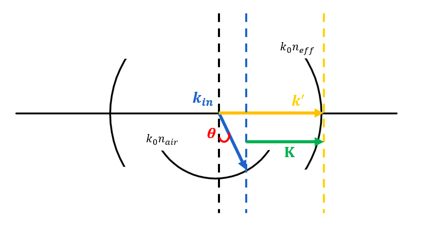
Using the k-diagram we drew above, we can easily write down such equation: $$ K=k^{’}-k_{in} sin\theta $$
As an initial design, we assume the duty cycle as 50%. Then we can get the effective index(\(n_{eff}\) in the software material library, which is around 1.4997 at 266nm. Combing with the K-vector: $$ K=\frac{2\pi}{\Lambda} $$
We can derive the period of the grating as follows: $$ \Lambda=\frac{\lambda}{n_{eff}-n_{air}sin\theta} $$
Substituting the values to calculate, we can get the period should be around 200nm.
Model Structure
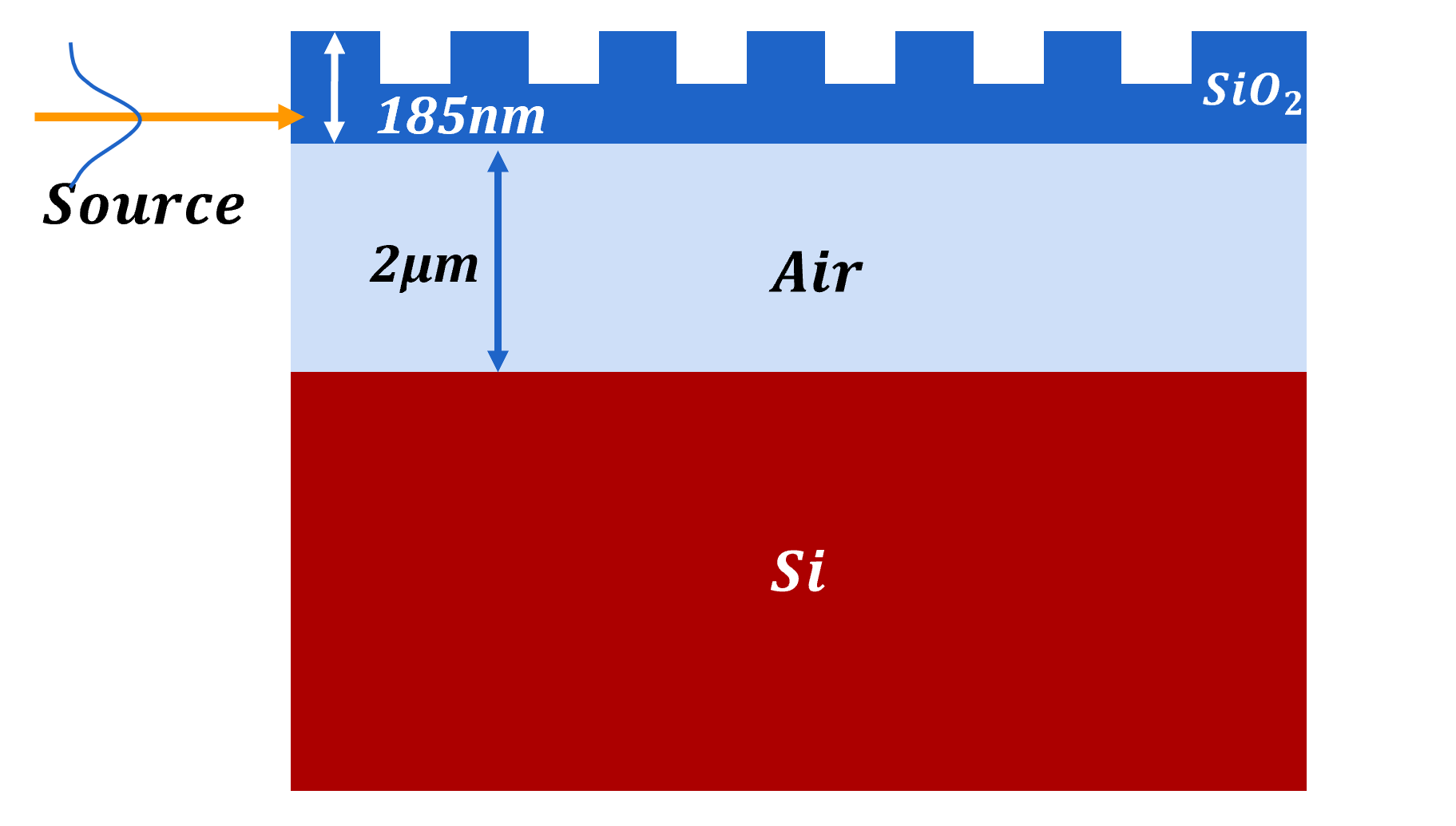
In the Lumerical software, we build a structure like the figure above. For the initial design, we choose the thickness of the grating waveguide as 185nm. Under the grating layer is 2µm air, then is a thick Si substrate.
While building the simulation model, we found it is not wise to put a source with a specific angle directly, it will introduce incident position as a new variable and it needs a large source scale to cover the whole grating which will lead longer time for simulating. So we utilize the reversibility of the optical path to change our minds to simulate, we put a source as incident light from the left of the grating and put a monitor just above the whole structure. In this way, we can collect all the light coupling from the waveguide to air without considering the incident position, and determine the coupling efficiency of the grating coupler.
Simulation Result
In the last chapter, we calculate and get the period of the grating. However, there are still other parameters that influence the coupling efficiency of the grating coupler. In this chapter, we want to study the effect of etch depth on coupling efficiency in different conditions, which means we need to fix other variables that will influence the coupling efficiency. To perfect our design, we need to start with the determination of the duty cycle, which is another important grating coupler parameter.
Initial simulation
First, we run the initial simulation, this is the simulation that works for determining some important parameters and ensures the following simulation results are valuable for our design goals. In this simulation, we set the duty cycle as 50% and sweep the coupling efficiency at different etch depths. The result is shown as follows:
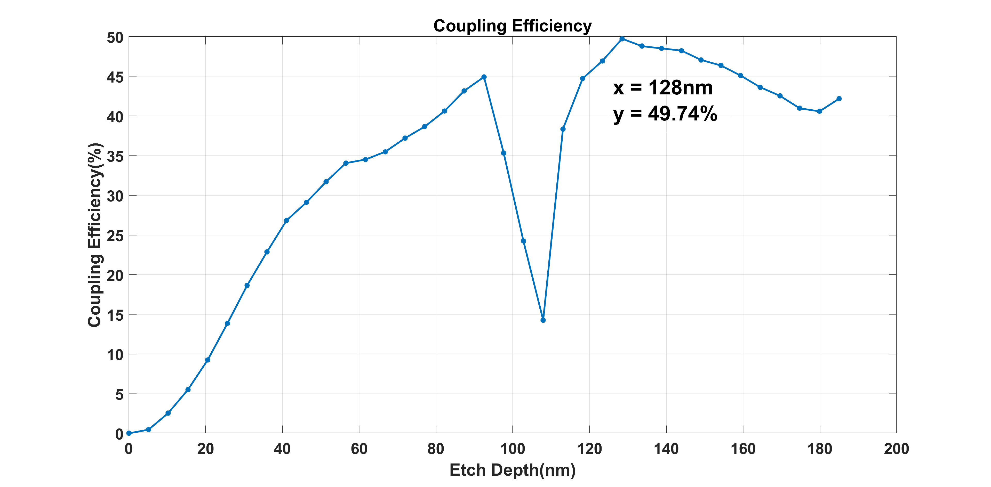
From the figure4, the first thing we noticed is the weird dip when the etch depth is close to 100nm. To explain that, we went through another two simulations and observed the cross-section E-field figure passing through the waveguide. Before that, I want to go into detail about the structure we simulated. This would be very helpful for understanding simulation results.
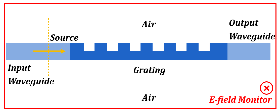
The above figure shows the structure we simulate in this section. Before and after the grating we have input and output waveguides, with the same thickness of the grating total. Then we put the fundamental source with wavelength at 266nm in the input waveguide. Above and below the structure are just air, and an E-field monitor covers the whole structure to see the propagation passing through the structure’s cross-section. We chose two groups of parameters to do the simulation, one is the most efficient point with 128nm etch depth, and the other one is the least efficient point with 107nm etch depth. Then we obtained these two figures:
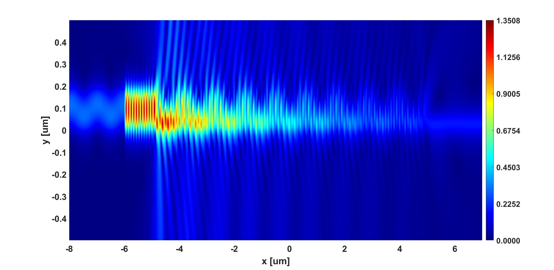
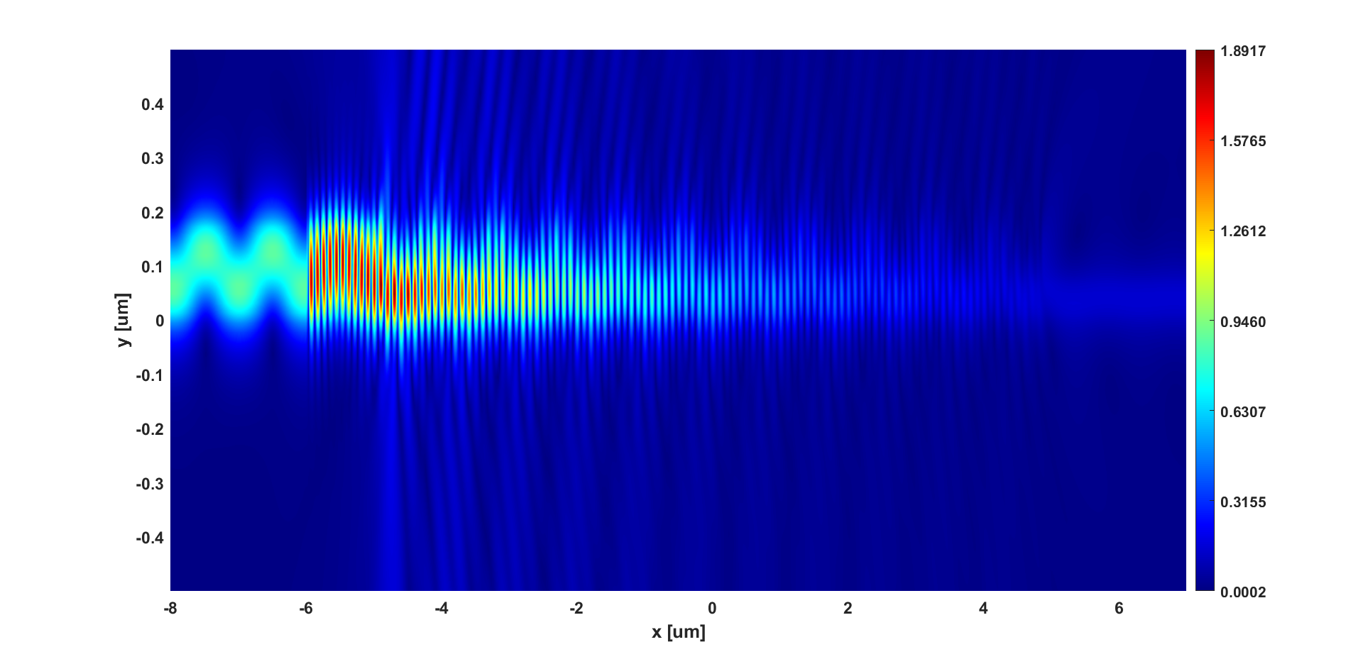
Comparing the two figures above, a much stronger back reflection can be observed clearly in the 107nm etch depth condition than in the 128nm etch depth condition. By putting a monitor behind the source, we can obtain how much light goes back, And the result says there are 67% of light goes back in 107nm etch depth condition, while for 128nm etch depth condition, the result is only about 9%. Furthermore, if we observe the patterns in these two figures, we can find the 107 etch depth condition forms a strong standing wave before the grating structure.
These phenomena all point to the same cause, in this etch depth, the effective index change forms a strong back reflection. Then the back reflected light interferes with the source and superimposes, making more light leak out from the back not being coupled by the grating. Reflected on the etch depth sweep image we get a visible dip in this range of etch depth.
Back to the etch depth sweep Figure4, another point we cared about is the point which has the most coupling efficiency. When the etch depth is 128nm, we got 49.74% coupling efficiency which seems good. However, considering the fabrication, this parameter means that after the etching process, the remaining part of the grating is only 57nm thick. This is not a good thickness because of the stress in the material. The entire structure may collapse due to its stress concentration, and the grating will break up. To avoid that, we thickened the whole thickness of the grating to 300nm and did the following optimization design.
Parameter optimization
Until now, we still haven’t got a proper value of the grating duty cycle. However, both changing the duty cycle and etch depth will change the coupling efficiency, which means that we need to sweep two parameters at the same time. Considering that we want to iterate as many times as possible in parameter optimization, a double sweep at the same time will cost extensive computing resources and time, a double sweep is not a good choice.
Based on such considerations, we used the optimization function in the Lumerical at first. The optimization function can change no matter how many parameters are at the same time, and give the “best of merit” in a proper number of iterations. Set the coupling efficiency as the ”merit” we want, the optimization function gives us a set of parameters. 150nm and 27% duty cycle is the best solution it found. Nevertheless, this function cannot show us a trend when the parameters change. To verify the result, we run another two sweeps.
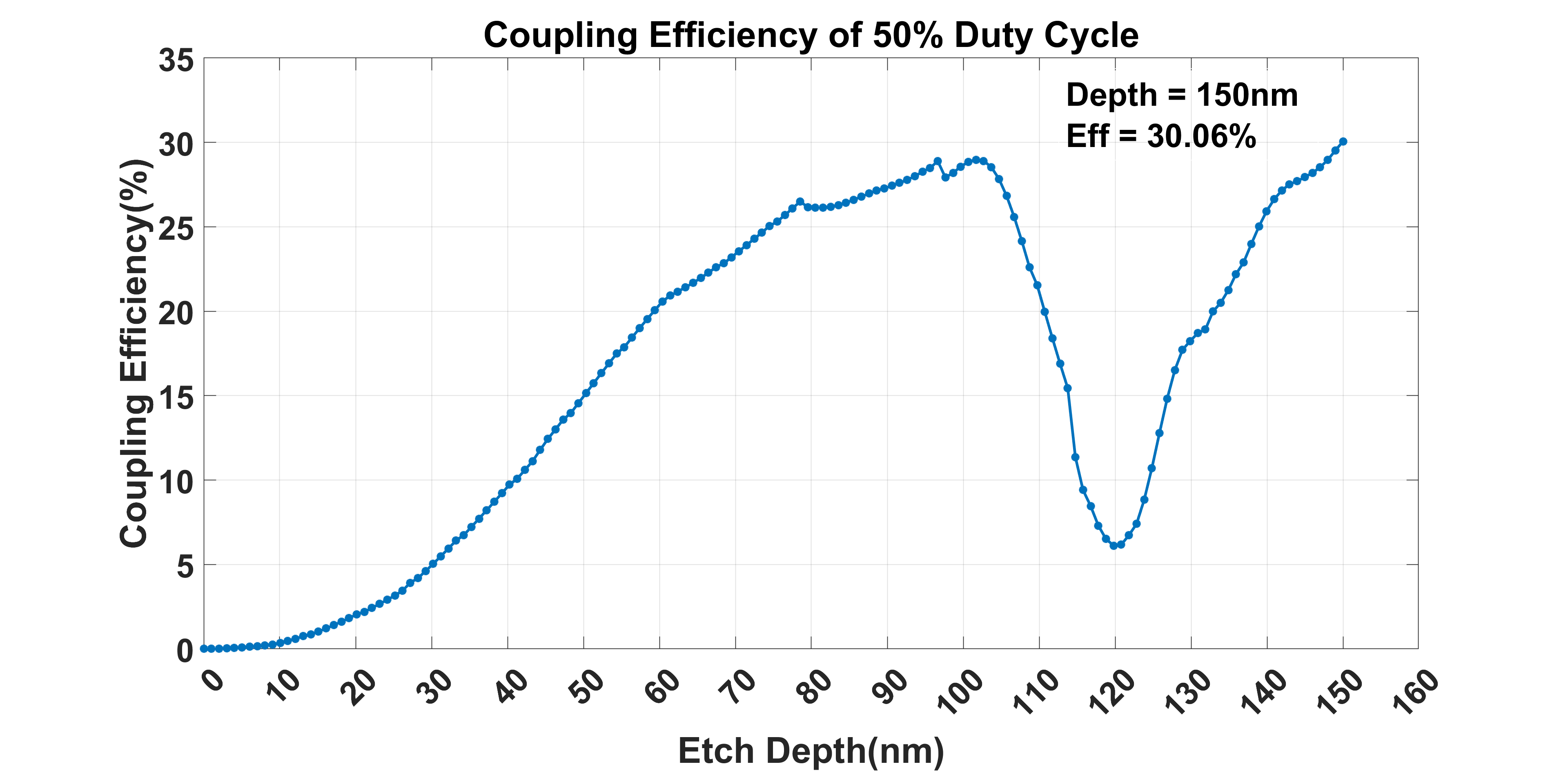
First, we still fix the duty cycle as 50%, then start to sweep the etch depth from 0 to 150nm. By this way after etching, we can still have 150nm remaining to ensure the strength of the structure. From the result above, we can find with a 50% duty cycle, 150nm etch depth is indeed the point which has the most coupling efficiency. With this conclusion, we fixed the etch depth as 150nm, then ran the sweep of duty cycle, and got the result as follows:
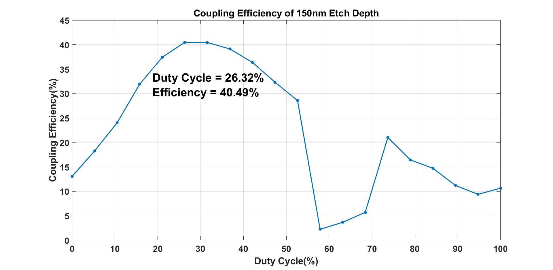
From the figure, we can observe the trend of the coupling efficiency changed by the duty cycle very clearly. When the duty cycle is around 30%, the coupling efficiency is very close. So for the following design and simulation, considering the process precision, we will use 30% as the duty cycle of the grating.
Absorption of Si
After determining the key parameters, we first did a simulation under a 30% duty cycle, 200nm period, 300nm grating thickness, and 10µm long to see how the etch depth influences the coupling efficiency.
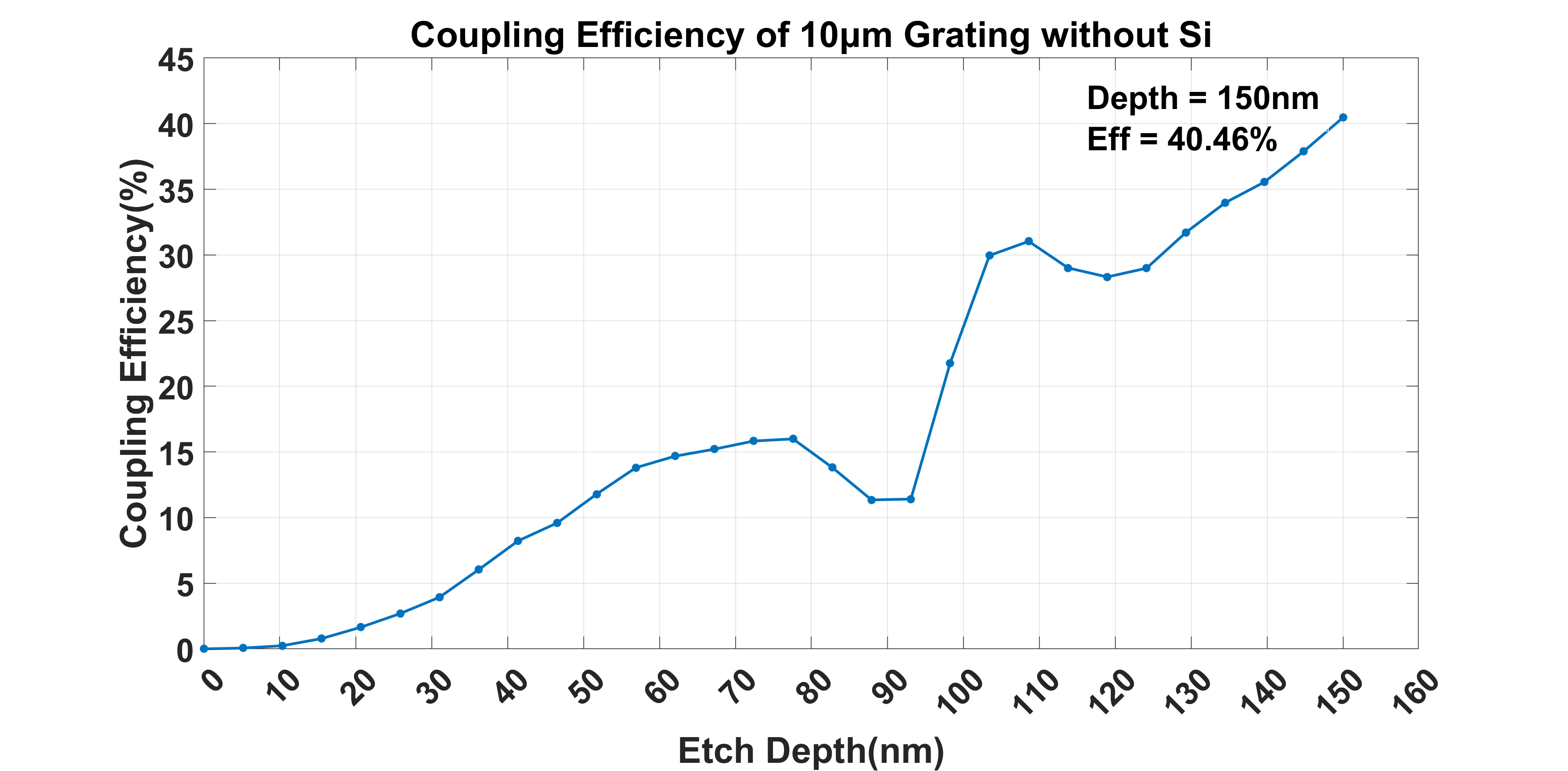
The largest coupling efficiency point is very close to the simulation we did in the first two steps. And curve looks a little similar to the first etch depth sweep figure4. There is a similar dip happens in the near 100nm etch depth range. And the reason we think is the same as the first one, which is caused by the back reflection.
In this condition, we put a power monitor around the structure. The top monitor is 10µm above the grating, to reduce the impact of the wave itself on the collection. It shows the coupling efficiency which is nearly 40% as the curve shows. A monitor placed at the end of the output waveguide records how much light just passes through the structure. This result is 26.07%. Then there is still a monitor which is placed behind the source to monitor back reflection. The back reflection for now is around 30.87%. At last, we put a monitor under the grating structure, which also has a 10µm distance from the grating bottom. This monitor collects only 1.08% of light. If we add these results together, we find that the resulting light is about 98% of the total light source. This is because part of the light is lost during propagation, and it also proves the accuracy of our simulation result.
To further optimize the design, we add 5µm Si as the substrate below the air layer. The thickness of the air below the grating is 2µm.
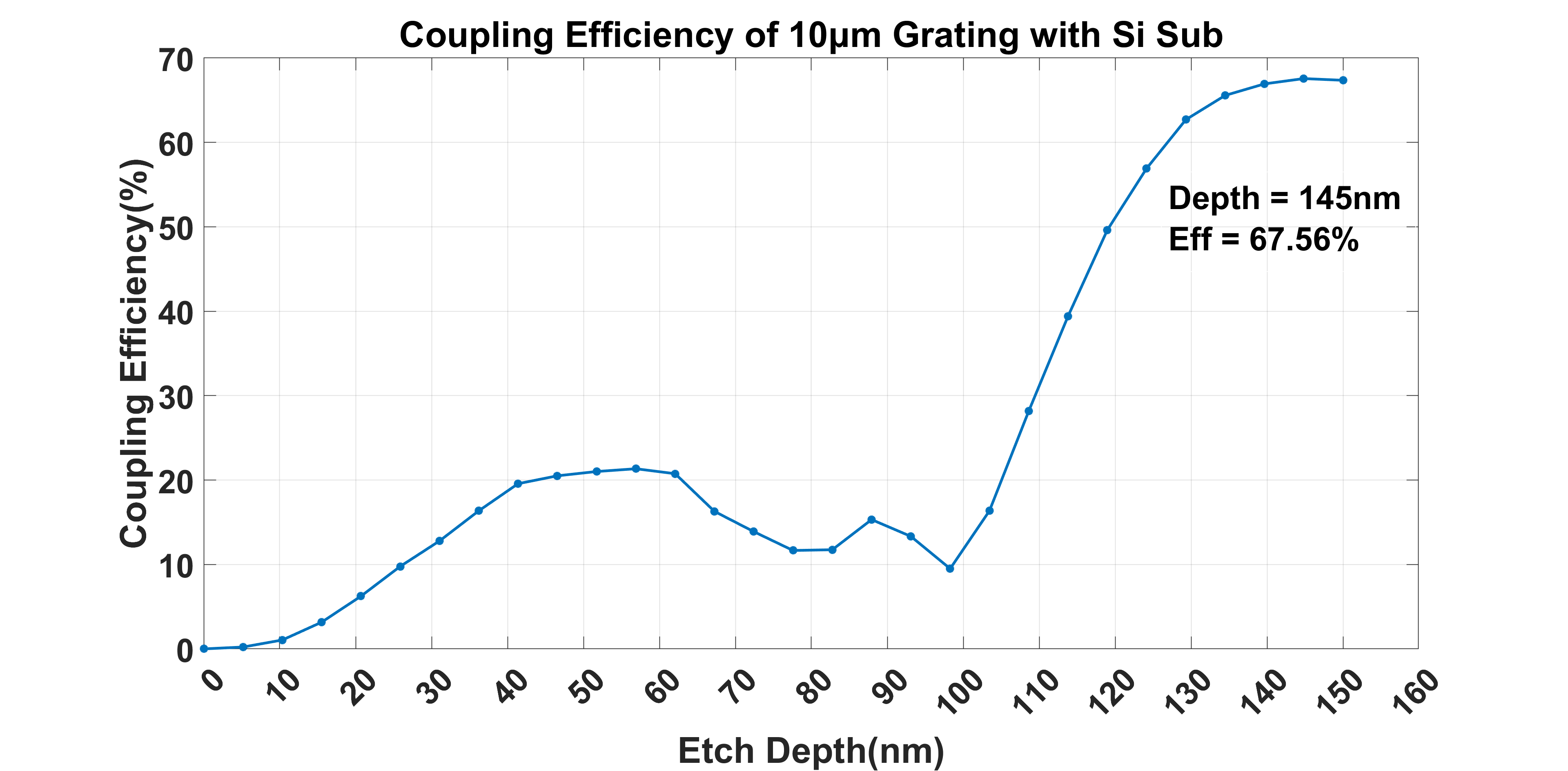
Although it still has a little dip like our first simulation, there has been a huge improvement in the coupling efficiency. Now with 145nm etch depth, the coupling efficiency can reach to 67.56%. Compared to 40% coupling efficiency at 150nm etch depth without Si substrate, we can notice a little etch depth shift between them. We think they are all the results of the influence of Si substrate.
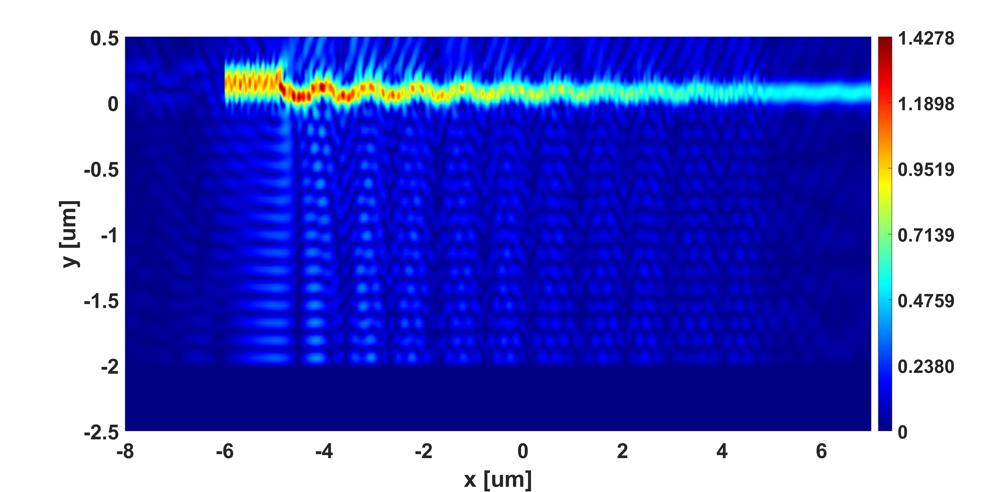
To confirm our conjecture, we build a cross-section view to monitor the electric field passing through the structure again. The figure we obtained is shown above. Si substrate works like a mirror, it’s obvious to see that the light is reflected back to the grating and coupled again. In this way, the coupling efficiency can be improved compared to the structure without Si substrate. As the Si doesn’t have 100% reflectivity, the light which doesn’t be reflected will be absorbed by the Si. That’s why we can see a dark range in the figure. That dark area indicates where the silicon substrate is located.
Grating Length
In the last section, we study the grating length influence. Fixed the period, duty cycle, grating thickness and materials as same to previous work, just lengthened the grating coupler to 50µm. Then still do the sweep on the etch depth, the result we got is the figure as follows.
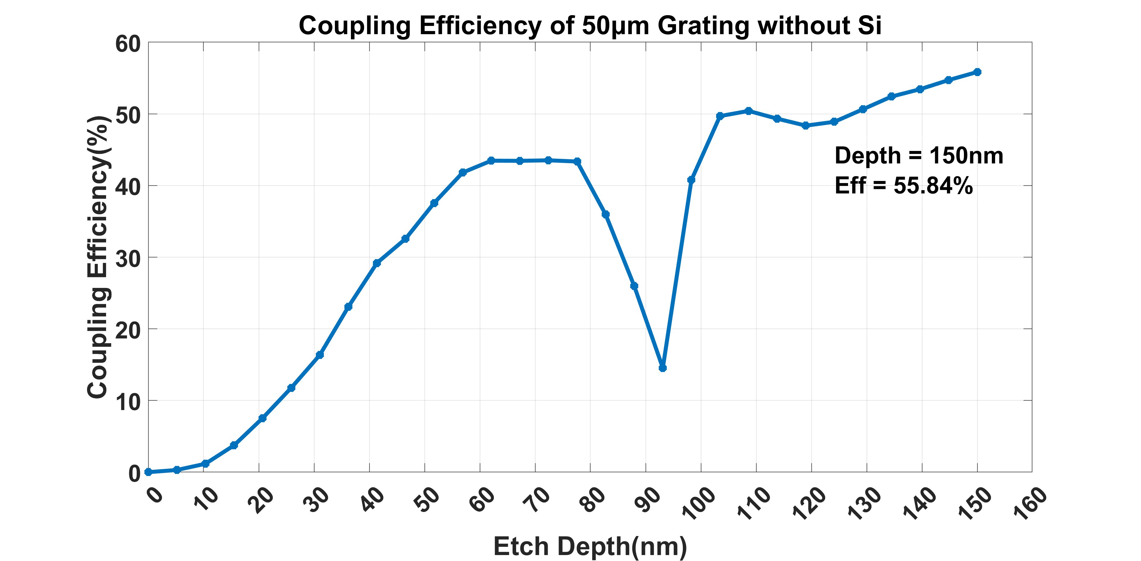
Observe the curve, the shape is still similar to the previous simulation. The dip in coupling efficiency still exists. This further confirms our conjecture, because the grating length won’t influence the effective refractive index. The dip is just the result of effective refractive index change, which forms a strong back reflection. When we lengthen the grating coupler length, this strong back reflection will still happen when the etch depth is close to 100nm.
Meanwhile, a longer grating coupler means more light can be coupled. That’s why we can find in some other parameters and the same etch depth at 150nm, a 50µm grating coupler has a coupling efficiency of 55.84%, which is much higher than the 40.46% of a 10µm grating coupler.
Conclusion
During this research on Ultra Violet C Irradiation grating coupler, we can make the following conclusions:
- Design different length grating couplers work at 266nm wavelength. The period of the grating coupler is 200nm, the duty cycle is 30%, etch depth is 150nm.
- This grating coupler can achieve around 40% coupling efficiency at 10µm long, and 55% at 50µm long.
- By adding a Si substrate 2µm below the air under the grating, the grating coupler can have a better performance. For a 10µm grating coupler, the Si substrate can increase coupling efficiency to 67%.
- During the design process, we should always be concerned about the fabrication. Ensure the structural strength will not be damaged, and the structure should be able to be fabricated.
- In some etch depth ranges, the change in effective refractive index will lead to strong back reflection. This will lead to a substantial drop in coupling efficiency.
Generally speaking, we basically completed the design work under the requirements of the design objectives.
References
[1] Susan Givens Bell. “Antibiotic resistance: is the end of an era near?” In: Neonatal Network 22.6 (2003), pp. 47–54.
[2] Manuel V´azquez and Arnold Hanslmeier. Ultraviolet radiation in the solar system. Vol. 331. Springer Science & Business Media, 2005.
[3] Walter Harm. “Biological effects of ultraviolet radiation”. In: (1980).
[4] Thomas A Klar and Stefan W Hell. “Subdiffraction resolution in far-field fluorescence microscopy”. In: Optics letters 24.14 (1999), pp. 954–956.
[5] MJ Rycroft. “Computational electrodynamics, the finite-difference time-domain method”. In: Journal of Atmospheric and Terrestrial Physics 15.58 (1996), pp. 1817–1818.
[6] Kane Yee. “Numerical solution of initial boundary value problems involving Maxwell’s equations in isotropic media”. In: IEEE Transactions on antennas and propagation 14.3 (1966), pp. 302–307.
[7] A Imre et al. “Multiplexing surface plasmon polaritons on nanowires”. In: Applied Physics Letters 91.8 (2007), p. 083115.
[8] Robert Halir et al. “Waveguide grating coupler with subwavelength microstructures”. In: Optics letters 34.9 (2009), pp. 1408–1410.
[9] Yun Wang et al. “Universal grating coupler design”. In: Photonics North 2013. Vol. 8915. SPIE. 2013, pp. 284–290.
[10] Theodor Tamir and Song-Tsuen Peng. “Analysis and design of grating couplers”. In: Applied physics 14 (1977), pp. 235–254.